Technology business briefs for February 24, 2017
Google Features Intel Skylake Xeons For Its Cloud Platform
Source: TweakTown
Google (GOOG) (GOOGL) announced today that it would be the first cloud provider to offer the "next generation Intel (NASDAQ:INTC) Xeon processor, codenamed Skylake." This follows the announcement of a strategic alliance with Intel to use the processors that was made back in November 2016.
While use of the new Intel processors was expected, perhaps what wasn't expected is how soon they will be available. Google says that customers will be able to see Xeon Skylakes "in action" at Google Cloud NEXT '17 on March 8.
At Intel's Investor Meeting, little was said about Xeon processor plans, except that Broadwell architecture-based Xeons would be upgraded to Skylake. No timeline was given. But the availability at the end of Q1 suggests that Intel has beaten Advanced Micro Devices' (AMD) Naples server chips to market by some months.
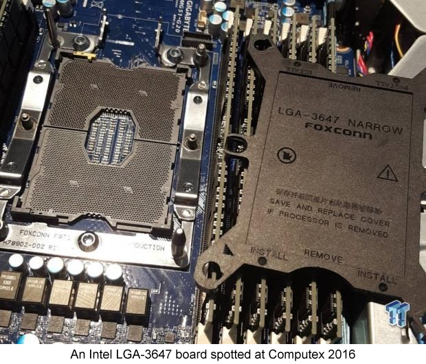
Presumably, these new Skylake Xeons will be the Xeon V5 processors that have been rumored for some time. These chips will feature yet another Intel LGA standard, LGA-3647 shown above, and feature as many as 28 CPU cores. They will be fabricated still on Intel's 14 nm process.
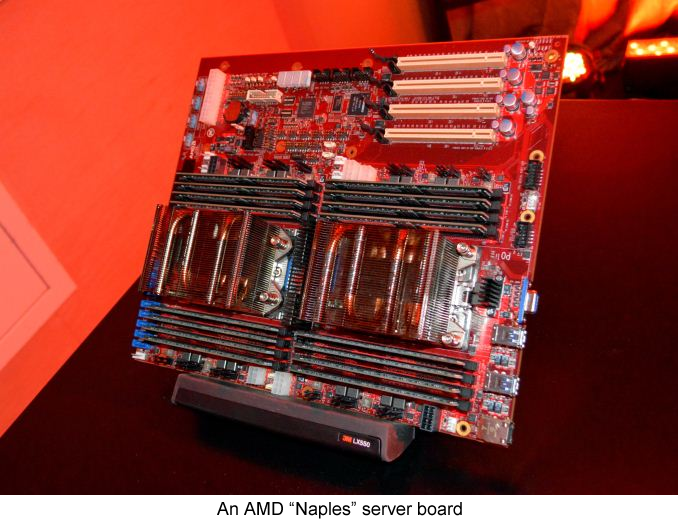
How Intel's Skylake Xeons will stack up in performance against the up to 32 core Naples remains to be seen. Engineering samples of Naples have been available since mid-August when a prototype server board mounting dual Naples chips was shown to the public.
Source: Anandtech
Almost certainly, AMD has tried to interest Google with Naples. Anandtech reported in August that development systems "are currently in the hands of select AMD partners for qualification and development." Apparently, Google wasn't impressed by what AMD had to offer, and chose to go with Intel when it announced its decision last November.
With the Google announcement, we see clearly Intel's modus operandi in dealing with AMD. There were no big product announcements or splashy media events. Everything was played very close to the vest. No information regarding release timing was given. Even the Investor Meeting contained very little for analysts to work with.
And Intel doesn't even make the announcement but leaves it to its partner to break the news. Intel appears to be targeting the large datacenter customers first with its chips before releasing them to server OEMs. This is a smart move because that's where the profitability and volume has shifted.
In case the reader hasn't noticed it, Intel is taking a page from the Nvidia (NVDA) playbook. When Nvidia first announced its Pascal GPUs, the first customers to receive them were not the graphics card OEMs but Nvidia's datacenter customers. Nvidia then worked its way down market, stopping first with its high-end desktop GPU, the GTX 1080, then releasing successively lower priced versions. This strategy may have cost Nvidia some market share in desktop add-in boards, but it allowed Nvidia to capture the most lucrative GPU markets.
The Google announcement shows how different Intel's tactics are compared to AMD's. AMD has marketed its Zen CPUs through various levels of previews, pre-announcements and finally product launches, all designed to build anticipation. Along the way, it has featured cherry-picked benchmarks that it claims to show that its products are superior to Intel. While such marketing helps sell AMD to investors and fans, it also affords AMD's competition considerable advance warning of AMD's product plans.
Intel has done almost the exact opposite, giving away very little of its product plans, basically playing possum. This has led some to believe that Intel has no response to AMD, but we're seeing with the Google announcement that Intel very definitely has a response, at least in its core growth area of the datacenter.
TSMC's 10 nm On Track
Taiwan Semiconductor Manufacturing Company (TSM) is currently ramping production of it 10 nm process. According to Digitimes, co-CEO Mark Liu, speaking at its annual supply chain management forum on February 23 gave assurances that the foundry will make its first commercial shipments on the new node later this quarter.
That's phenomenally good progress and also good news for TSMC's key customer, Apple (AAPL). I've been saying for some time that Apple would use TSMC's 10 nm process for its next generation systems on chip, which will probably be called the A11. Based on the timing of availability, clearly, these chips will be featured in the iPhone 8.
It's also thought that the 10 nm process could be used for a forthcoming iPad refresh rumored to be some time in March. This rumor is probably a little softer since it is at variance with Apple's usual development process. In the past, as in the case of the A9 of the iPhone 6s, this was followed by the A9X, which has been featured in the iPad Pros. So I consider it a little more likely that the iPad refresh, if it comes this spring, will feature an "A10X" processor fabricated on TSMC's 16 nm node, as the A10 currently is. But if Apple switches to 10 nm for the iPad refresh, it could help boost iPad sales.
Other potential customers for TSMC's 10 nm process include Nvidia. Nvidia has provided sneak peaks of its Xavier single board solution for autonomous vehicles. The Xavier processor features a next-generation Volta architecture GPU section on the SOC. Xavier is being touted as a much more energy efficient solution than Nvidia's current Drive PX 2 system, which uses two Parker SOCs and two Pascal architecture GPUs. Xavier would be a good candidate for 10 nm.
Nvidia also has an interest in moving its discrete GPU lineup (currently Pascal architecture fabbed on TSMC's 16 nm) to Volta. Whether Volta will be fabricated on 10 nm or 16 nm continues to be a subject of lively debate. Volta was originally intended for 10 nm when it first appeared in Nvidia's GPU roadmap, but that was before Pascal was inserted.
I think it's mainly a matter of availability. Apple may simply take all the 10 nm production available from TSMC, leaving nothing for other potential customers. With the impending arrival of AMD's Vega GPUs, Nvidia could be forced to build Volta on an "improved" TSMC 16 nm node, which some have called a "12 nm" node, following comments made at TSMC's Q4 earnings teleconference.
Samsung's Exynos 9 Ready for Mobile World Congress
With Mobile World Congress (MWC) about to start in Barcelona on February 27, Samsung (OTCPK:SSNLF) has unveiled its Exynos 9 mobile SOC, which will be fabricated on its own 10 nm process. The processor will feature an 8 core design using four of Samsung's custom M2 cores along with four Cortex-A53 cores. The chip will also have a built-in Samsung-designed LTE modem with download speeds up to 1 Gbps.
The SOC will also feature advanced camera features such as support for dual rear-facing cameras and 4K video record and playback at up to 120 fps. The SOC also features a "separate processing unit" for enhanced security and mobile payments. This sounds very much like the Secure Enclave processor that Apple embeds in its SOCs.
All of this is by way of setting up for the usual flagship Galaxy smartphone launch that Samsung does at MWC. It's expected that the next Galaxy (S8) will use the Exynos 9 in international markets while the S8 will use Qualcomm's (QCOM) Snapdragon 835 processor in the US and possibly in China. The Snapdragon 835 has already been announced and will be fabbed using Samsung's 10 nm process as well.
Note to readers: Beginning March 1, I'll be starting a new Marketplace service. At that point, my full articles will only be available by subscription.
I will continue to publish a daily newsletter/tech digest such as this article that will be available for free on SA. I'll continue to test and evolve this "digest" format in the coming days leading up to the launch of the service. To read more about the subscription service and my reasons for starting it, see my Instablog post.