We looked at Atomera (NASDAQ:ATOM) in June and noted that the company, which developed a technology called MST for speeding up transistors, achieved a technical break-through and was gaining traction with chip designers trying out its technology.
We briefly described the MST technology in our previous article, but a much more comprehensive take comes from SA contributor Vision and Value, which we highly recommend for those interested in how the MST technology works and how it fits in the semiconductor industry.
The company has really substantial IP. Over the last 12 months, it has grown its number of patents granted and pending from 184 to 230.
The earnings model is as follows. From the earnings deck:
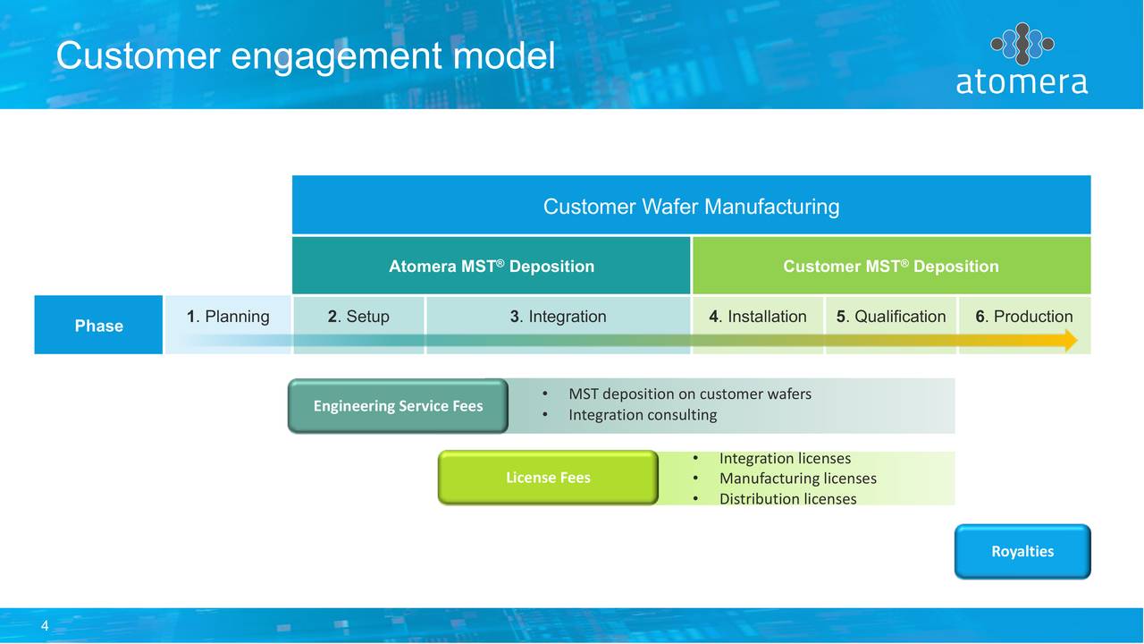
Customers can be distinguished into five phases. From the Q3CC (our emphasis):
Phase 1 includes customers under NDA who are planning an evaluation of our technology. In phase 2 we deposit MST film on customers' wafers and conduct physical characterization. Phase 3 is where customers incorporate MST on their wafers during an R&D run in their fab and use the test results to justify licensing our technology. It is generally in Phase 3 that we are most likely to sign integration licenses with customers. Phase 4 where customers execute a manufacturing license and install MST on EPI tool in their fab and in Phase 5 customers get a distribution license and transition to production.
Below you can see how the number of customers in the different phases is growing (earnings deck):

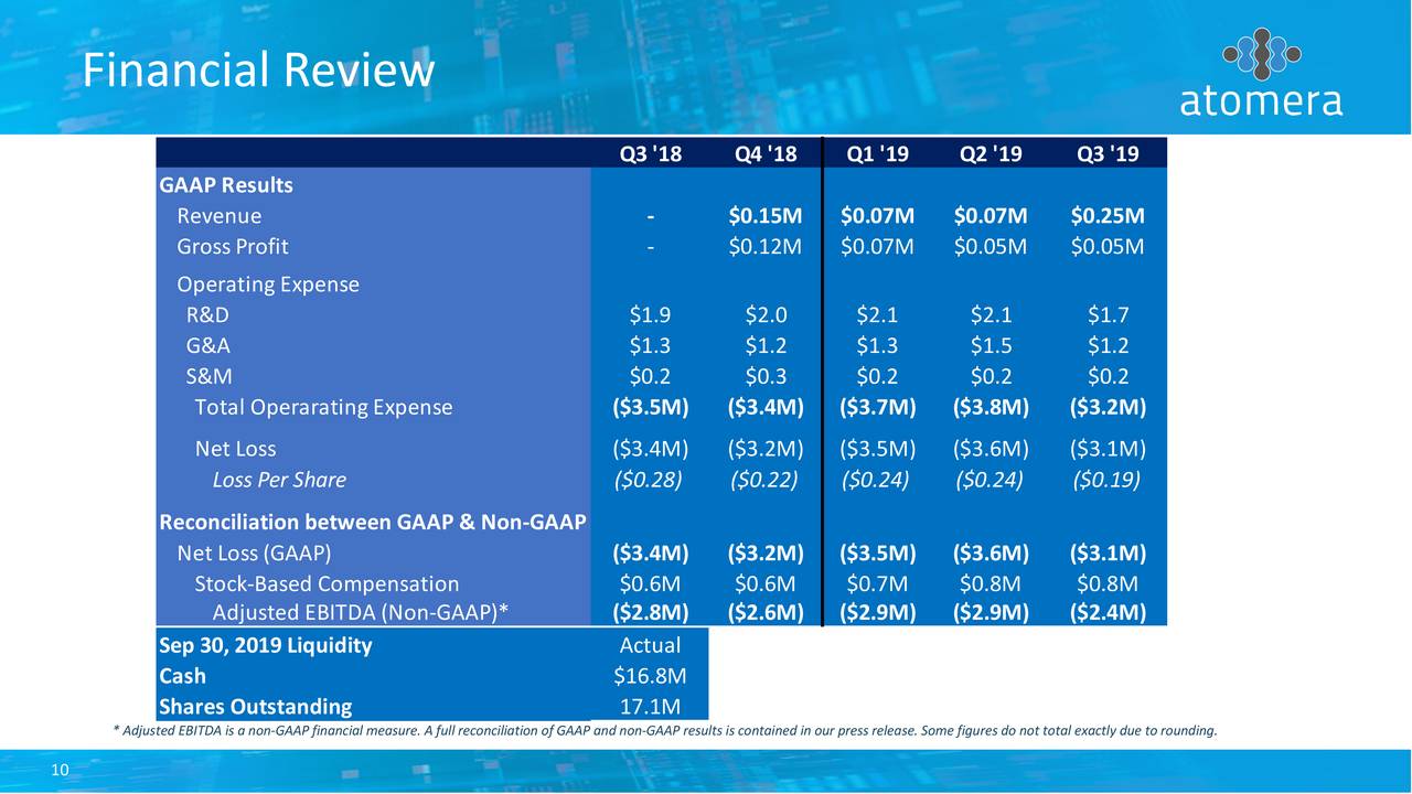
With at least 50% of the top semiconductor companies somewhere in this graph as customers in different phases, one might wonder why the company is earning so little revenue still. From the earnings deck:
There are several categories of revenues:
- Engineering services revenue from customers conducting MST deposition runs.
- Upfront revenue for integration, manufacturing